This chapter has been viewed 3461 times.Design Systems
The sequence of steps for FPGA design is similar to the sequence discussed in Section 1.2, “Design Flow”. As for any ASIC a designer needs design-entry software, a cell library, and physical-design software. Each of the FPGA vendors sells design kits that include all the software and hardware that a designer needs. Many of these kits use design-entry software produced by a different company. Often designers buy that software from the FPGA vendor. This is called an original equipment manufacturer(OEM) arrangement—similar to buying a car with a stereo manufactured by an electronics company but labeled with the automobile company’s name. Design entry uses cell libraries that are unique to each FPGA vendor. All of the FPGA vendors produce their own physical-design software so they can tune the algorithms to their own architecture.
Unfortunately, there are no standards in FPGA design. Thus, for example, Xilinx calls its 2:1 MUX an M2_1 with inputs labeled D0, and S0 with output O. Actel calls a 2:1 MUX an MX2 with inputs A, B, and S with output Y. This problem is not peculiar to Xilinx and Actel; each ASIC vendor names its logic cells, buffers, pads, and so on in a different manner. Consequently designers may not be able to transfer a netlist using one ASIC vendor library to another. Worse than this, designers may not even be able to transfer a design between two FPGA families made by the same FPGA vendor!
One solution to the lack of standards for cell libraries is to use a generic cell library, independent from any particular FPGA vendor. For example, most of the FPGA libraries include symbols that are equivalent to TTL 7400 logic series parts. The FPGA vendor’s own software automatically handles the conversion from schematic symbols to the logic cells of the FPGA.
Schematic entry is not the only method of design entry for FPGAs. Some designers are happier describing control logic and state machines in terms of state diagrams and logic equations. A solution to some of the problems with schematic entry for FPGA design is to use one of several hardware description languages (HDLs) for which there are some standards. There are two sets of languages in common use. One set has evolved from the design of programmable logic devices (PLDs). The ABEL (pronounced “able”), CUPL (“cupple”), and PALASM (“pal-azzam”) languages are simple and easy to learn. These languages are useful for describing state machines and combinational logic. The other set of HDLs includes VHDL and Verilog, which are higher-level and are more complex but are capable of describing complete ASICs and systems.
After completing design entry and generating a netlist, the next step is simulation. Two types of simulators are normally used for FPGA design. The first is a logic simulator for behavioral, functional, and timing simulation. This tool can catch any design errors. The designer provides input waveforms to the simulator and checks to see that the outputs are as expected. At this point, using a nondeterministic architecture, logic path delays are only estimates, since the wiring delays will not be known until after physical design (place-and-route) is complete. Designers then add or back-annotate the postlayout timing information to the postlayout netlist (also called a back-annotated netlist). This is followed by a postlayout timing simulation.
The second type of simulator, the type most often used in FPGA design, is a timing-analysis tool. A timing analyzer is a static simulator and removes the need for input waveforms. Instead the timing analyzer checks for critical paths that limit the speed of operation—signal paths that have large delays caused, say, by a high fanout net. Designers can set a certain delay restriction on a net or path as a timing constraint; if the actual delay is longer, this is a timing violation. In most design systems we can return to design entry and tag critical paths with attributes before completing the place-and-route step again. The next time we use the place-and-route software it will pay special attention to those signals we have labeled as critical in order to minimize the routing delays associated with those signals. The problem is that this iterative process can be lengthy and sometimes nonconvergent. Each time timing violations are fixed, others appear. This is especially a problem with place-and-route software that uses random algorithms (and forms a chaotic system). More complex (and expensive) logic synthesizers can automate this iterative stage of the design process. The critical path information is calculated in the logic synthesizer, and timing constraints are created in a feedforward path (this is called forward-annotation ) to direct the place-and-route software.
Although some FPGAs are reprogrammable, it is not a good idea to rely on this fact. It is very tempting to program the FPGA, test it, make changes to the netlist, and then keep programming the device until it works. This process is much more time consuming and much less reliable than performing thorough simulation. It is quite possible, for example, to get a chip working in an experimental fashion without really knowing why. The danger here is that the design may fail under some other set of operating conditions or circumstances. Simulation is the proper way to catch and correct these potential disasters.
8.1.1 Xilinx
Figure 8.1 shows the Xilinx design system. Using third-party design-entry software, the designer creates a netlist that forms the input to the Xilinx software. Utility software ( pin2xnf for FutureNet DASH and wir2xnf for Viewlogic, for example) translate the netlist into a Xilinx netlist format ( XNF ) file. In the next step the Xilinx program xnfmap takes the XNF netlist and maps the logic into the Xilinx Logic Cell Array ( LCA ) architecture. The output from the mapping step is a MAP file. The schematic MAP file may then be merged with other MAP files using xnfmerge . This technique is useful to merge different pieces of a design, some created using schematic entry and others created, for example, using logic synthesis. A translator program map2lca translates from the logic gates (NAND gates, NOR gates, and so on) to the required CLB configurations and produces an unrouted LCA file. The Xilinx place-and-route software ( apr or ppr ) takes the unrouted LCA file and performs the allocation of CLBs and completes the routing. The result is a routed LCA file. A control program xmake (that works like the make program in C) can automatically handle the mapping, merging, and place-and-route steps. Following the place-and-route step, the logic and wiring delays are known and the postlayout netlist may be generated. After a postlayout simulation the download file or BIT file used to program the FPGA (or a PROM that will load the FPGA) is generated using the Xilinx makebits program.
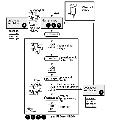 |
| FIGURE 8.1 The Xilinx FPGA design flow. The numbers next to the steps in the flow correspond to those in the general ASIC design flow of Figure 1.10 . |
Xilinx also provides a software program (Xilinx design editor, XDE) that permits manual control over the placement and routing of a Xilinx FPGA. The designer views a graphical representation of the FPGA, showing all the CLBs and interconnect, and can make or alter connections by pointing and clicking. This program is useful to check an automatically generated layout, or to explore critical routing paths, or to change and hand tune a critical connection, for example.
Xilinx uses a system called X-BLOX for creating regular structures such as vectored instances and datapaths. This system works with the Xilinx XNF netlist format. Other vendors, notably Actel and Altera, use a standard called Relationally Placed Modules ( RPM ), based on the EDIF standard, that ensures that the pieces of an 8-bit adder, for example, are treated as a macro and stay together during placement.
8.1.2 Actel
Actel FPGA design uses third-party design entry and simulators. After creating a netlist, a designer uses the Actel software for the place-and-route step. The Actel design software, like other FPGA and ASIC design systems, employs a large number of file formats with associated filename extensions. Table 8.1 shows some of the Actel file extensions and their meanings.
| TABLE 8.1 File types used by Actel design software. | |
| ADL | Main design netlist |
| IPF | Partial or complete pin assignment for the design |
| CRT | Net criticality |
| VALIDATED | Audit information |
| COB | List of macros removed from design |
| VLD | Information, warning, and error messages |
| PIN | Complete pin assignment for the design |
| DFR | Information about routability and I/O assignment quality |
| LOC | Placement of non-I/O macros, pin swapping, and freeway assignment |
| PLI | Feedback from placement step |
| SEG | Assignment of horizontal routing segments |
| STF | Back-annotation timing |
| RTI | Feedback from routing step |
| FUS | Fuse coordinates (column-track, row-track) |
| DEL | Delays for input pins, nets, and I/O modules |
| AVI | Fuse programming times and currents for last chip programmed |
Actel software can also map hardware description files from other programmable logic design software into the Actel FPGA architecture. As an example, Table 8.2 shows a text description of a state machine using an HDL from a company called LOG/iC. You can then convert the LOG/iC code to the PALASM code shown in Table 8.2 . The Actel software can take the PALASM code and merge it with other PALASM files or netlists.
| TABLE 8.2 FPGA state-machine language. | |
| LOG/iC state-machine language | PALASM version |
| *IDENTIFICATIONsequence detector
LOG/iC code *X-NAMES X; !input *Y-NAMES D; !output, D = 1 when three 1’s appear on X *FLOW-TABLE ;State, X input, Y output, next state S1, X1, Y0, F2; S1, X0, Y0, F1; S2, X1, Y0, F3; S2, X0, Y0, F1; S3, X1, Y0, F4; S3, X0, Y0, F1; S4, X1, Y1, F4; S4, X0, Y0, F1; *STATE-ASSIGNMENT BINARY; *RUN-CONTROL PROGFORMAT = P-EQUATIONS; *END |
TITLE sequence detectorCHIP MEALY USER
CLK Z QQ2 QQ1 X EQUATIONS Z = X * QQ2 * QQ1 QQ2 := X * QQ1 + X * QQ2 QQ1 := X * QQ2 + X * /QQ1
|
8.1.3 Altera
Altera uses a self-contained design system for its complex PLDs that performs design entry, simulation, and programming of the parts. Altera also provides an input and output interface to EDIF so that designers may use third-party schematic entry or a logic synthesizer. We have seen that the interconnect scheme in the Altera complex PLDs is nearly deterministic, simplifying the physical-design software as well as eliminating the need for back-annotation and a postlayout simulation. As Altera FPGAs become larger and more complex, there are some exceptions to this rule. Some special cases require signals to make more than one pass through the routing structures or travel large distances across the Altera FastTrack interconnect. It is possible to tell if this will be the case only by trying to place and route an Altera device.
8.2 Logic Synthesis
Designers are increasingly using logic synthesis as a replacement for schematic entry. As microelectronic systems and their ASICs become more complex, the use of schematics becomes less practical. For example, a complex ASIC that contains over 10,000 gates might require hundreds of pages of schematics at the gate level. As another example, it is easier to write A = B + C than to draw a schematic for a 32-bit adder at the gate level.
The term logic synthesis is used to cover a broad range of software and software capabilities. Many logic synthesizers are based on logic minimization. Logic minimization is usually performed in one of two ways, either using a set of rules or using algorithms. Early logic-minimization software was designed using algorithms for two-level logic minimization and developed into multilevel logic-optimization software. Two-level and multilevel logic minimization is well suited to random logic that is to be implemented using a CBIC, MGA, or PLD. In these technologies, two-level logic can be implemented very efficiently. Logic minimization for FPGAs, including complex PLDs, is more difficult than other types of ASICs, because of the complex basic logic cells in FPGAs.
There are two ways to use logic synthesis in the design of FPGAs. The first and simplest method takes a hardware description, optimizes the logic, and then produces a netlist. The netlist is then passed to software that maps the netlist to an FPGA architecture. The disadvantage of this method is the inefficiency of decoupling the logic optimization from the mapping step. The second, more complicated, but more efficient method, takes the hardware description and directly optimizes the logic for a specific FPGA architecture.
Some logic synthesizers produce files in PALASM, ABEL, or CUPL formats. Software provided by the FPGA vendor then take these files and maps the logic to the FPGA architecture. The FPGA mapping software requires detailed knowledge of the FPGA architecture. This makes it difficult for third-party companies to create logic synthesis software that can map directly to the FPGA.
A problem with design-entry systems is the difficulty of moving netlists between different FPGA vendors. Once you have completed a design using an FPGA cell library, for example, you are committed to using that type of FPGA unless you repeat design entry using a different cell library. ASIC designers do not like this approach since it exposes them to the mercy of a single ASIC vendor. Logic synthesizers offer a degree of independence from FPGA vendors (universally referred to vendor independence, but this should, perhaps, be designer independence) by delaying the point in the design cycle at which designers need to make a decision on which FPGA to use. Of course, now designers become dependent on the synthesis software company.
8.2.1 FPGA Synthesis
For low-level logic synthesis, PALASM is a de facto standard as the lowest-common-denominator interchange format. Most FPGA design systems are capable of converting their own native formats into a PALASM file. The most common programmable logic design systems are ABEL from Data I/O, CUPL from P-CAD, LOG/iC from IsData, PALASM2 from AMD, and PGA-Designer from Minc. At a higher level, CAD companies (Cadence, Compass, Mentor, and Synopsys are examples) support most FPGA cell libraries. This allows you to map from a VHDL or Verilog description to an EDIF netlist that is compatible with FPGA design software. Sometimes you have to buy the cell library from the software company, sometimes from the FPGA vendor.
| TABLE 8.3 The VHDL code for the sequence detector of Table 8.2 . |
| entity detector is port (X, CLK: in BIT; Z : out BIT); end;architecture behave of SEQDET is
type STATES is (S1, S2, S3, S4); signal current, next: STATES; begin combinational: process begin case current is when S1 => if X = ‘1’ then Z <= ‘0’; next <= S3; else Z <= ‘0’; next <= S1; end if; when S2 => if X = ‘1’ then Z <= ‘0’; next <= S2; else Z <= ‘0’; next <= S1; end if; when S3 => if X = ‘1’ then Z <= ‘0’; next <= S2; else Z <= ‘0’; next <= S1; end if; when S4 => if X = ‘1’ then Z <= ‘1’; next <= S4; else Z <= ‘0’; next <= S1; end if end case; end process sequential: process begin wait until CLK’event and CLK = ‘1’; current <= next ; end process; end behave; |
As an example, Table 8.3 shows a VHDL model for a pattern detector to check for a sequence of three ‘1’s (excluding the code for the I/O pads). Table 8.4 shows a script or command file that runs the Synopsys software to generate an EDIF netlist from this VHDL that targets the TI version of the Actel FPGA parts. A script is a recipe that tells the software what to do. If we wanted to retarget this design to another type of FPGA or an MGA or CBIC ASIC, for example, we may only need a new set of cell libraries and to change the script (if we are lucky). In practice, we shall probably find we need to make a few changes in the VHDL code (in the areas of I/O pads, for example, that are different for each kind of ASIC). We now have a portable design and a measure of vendor independence. We have also introduced some dependence on the Synopsys software since the code in Table 8.3 might be portable, but the script (which is just as important a part of the design) in Table 8.4 may only be used with the Synopsys software. Nevertheless, using logic synthesis results in a more portable design than using schematic entry.
| TABLE 8.4 The Synopsys script for the VHDL code of Table 8.3. | |
| /design checking/search_path = .
/use the TI cell libraries/ link_library = tpc10.db target_library = tpc10.db symbol_library = tpc10.sdb read -f vhdl detector.vhd current_design = detector write -n -f db -hierarchy -0 detector.db check_design > detector.rpt |
report_design > detector.rpt/optimize for area/
max_area 0.0 compile write -h -f db -o detector_opt.db report -area -cell -timing > detector.rpt free -all /write EDIF netlist/ write -h -f edif -0 exit |
8.3 The Halfgate ASIC
This section illustrates FPGA design using a very simple ASIC—a single inverter. The hidden details of the design and construction of this “halfgate FPGA” are quite complicated. Fortunately, most of the inner workings of the design software are normally hidden from the designer. However, when software breaks, as it sometimes does, it is important to know how things work in order to fix the problem. The formats, filenames, and flow will change, but the information needed at each stage and the order in which it is conveyed will stay much the same.
8.3.1 Xilinx
Table 8.5 shows an FPGA design flow using Compass and Xilinx software. On the left of Table 8.5 is a script for the Compass programs—scripts for Cadence, Mentor, and Synopsys software are similar, but not all design software has the capability to be run on autopilot using scripts and a command language. The diagrams in Table 8.5 illustrate what is happening at each of the design steps. The following numbered comments, corresponding to the labels in Table 8.5, highlight the important steps:
| TABLE 8.5 Design flow for the Xilinx implementation of the halfgate ASIC. | |
| Script | Design flow |
| # halfgate.xilinx.inp
shell setdef path working xc4000d xblox cmosch000x quit asic open [v]halfgate synthesize save [nls]halfgate_p quit fpga set tag xc4000 set opt area optimize [nls]halfgate_p quit qtv open [nls]halfgate_p trace critical print trace [txt]halfgate_p quit shell vuterm exec xnfmerge -p 4003PC84 halfgate_p > /dev/null exec xnfprep halfgate_p > /dev/null exec ppr halfgate_p > /dev/null exec makebits -w halfgate_p > /dev/null exec lca2xnf -g -v halfgate_p halfgate_b > /dev/null quit manager notice utility netlist open [xnf]halfgate_b save [nls]halfgate_b save [edf]halfgate_b quit qtv open [nls]halfgate_b trace critical print trace [txt]halfgate_b quit
|
|
| TABLE 8.6 The Xilinx files for the halfgate ASIC. |
| Verilog file (halfgate.v) |
| Preroute XNF file (halfgate_p.xnf) |
| LCA file (halfgate_p.lca) |
| Postroute XNF file (halfgate_b.xnf) |
- The Verilog code, in halfgate.v , describes a single inverter.
- The script runs the logic synthesizer that converts the Verilog description to an inverter (using elements from the Xilinx XC4000 library) and saves the result in a netlist, halfgate_p.nls (a Compass internal format).
- The script next runs the logic optimizer for FPGAs. This program also adds the I/O pads. In this case, logic optimization implements the inverter by using an inverting output pad. The software writes out the netlist as halfgate_p.xnf .
- A timing simulation is run on the netlist halfgate_p.nls (the Compass format netlist). This netlist uses the default delays—every gate has a delay of 1 ns.
- At this point the script has run all of the Xilinx programs required to complete the place-and-route step. The Xilinx programs have created several files, the most important of which is halfgate_p.lca , which describes the FPGA layout. This postroute netlist is converted to halfgate_b.nls (the added suffix ‘b’ stands for back-annotation). Next a timing simulation is performed on the postroute netlist, which now includes delays, to find the delay from the input ( myInput ) to the output ( myOutput ). This is the critical—and only—path. The simulation (not shown) reveals that the delay is 2.8 ns (for the input buffer) plus 11.6 ns (for the output buffer), for a total delay of 14.4 ns (this is for a XC4003 in a PC84 package, and default speed grade ‘4’).
Table 8.6 shows the key Xilinx files that are created. The preroute file, halfgate_p.xnf , describes the IBUF and OBUF library cells but does not contain any delays. The LCA file, halfgate_p.lca , contains all the physical design information, including the locations of the pads and I/O cells on the FPGA ( PAD61 for myInput and PAD1 for myOutput ), as well as the details of the programmable connections between these I/O Cells. The postroute file, halfgate_b.xnf , is similar to the preroute version except that now the delays are included. Xilinx assigns delays to a pin (connector or terminal of a cell). In this case 2.8 ns is assigned to the output of the input buffer, 8.6 ns is assigned to the input of the output buffer, and finally 3.0 ns is assigned to the output of the output buffer.
8.3.2 Actel
The key Actel files for the halfgate design are the netlist file, halfgate_io.adl, and the STF delay file for back-annotation, halfgate_io.stf. Both of these files are shown in Table 8.7 (the STF file is large and only the last few lines, which contain the delay information, are shown in the table).
| TABLE 8.7 The Actel files for the halfgate ASIC. | |
| ADL file | STF file |
| ; HEADER; FILEID ADL ./halfgate_io.adl 85e8053b
; CHECKSUM 85e8053b ; PROGRAM certify ; VERSION 23/1 ; ALSMAJORREV 2 ; ALSMINORREV 3 ; ALSPATCHREV .1 ; NODEID 72705192 ; VAR FAMILY 1400 ; ENDHEADER DEF halfgate_io; myInput, myOutput. USE ADLIB:INBUF; INBUF_2. USE ADLIB:OUTBUF; OUTBUF_3. USE ADLIB:INV; u2. NET DEF_NET_8; u2:A, INBUF_2:Y. NET DEF_NET_9; myInput, INBUF_2:PAD. NET DEF_NET_11; OUTBUF_3:D, u2:Y. NET DEF_NET_12; myOutput, OUTBUF_3:PAD. END. |
; HEADER; FILEID STF ./halfgate_io.stf c96ef4d8
… lines omitted … (126 lines total)
DEF halfgate_io. USE ; INBUF_2/U0; TPADH:’11:26:37′, TPADL:’13:30:41′, TPADE:’12:29:41′, TPADD:’20:48:70′, TYH:’8:20:27′, TYL:’12:28:39′. PIN u2:A; RDEL:’13:31:42′, FDEL:’11:26:37′. USE ; OUTBUF_3/U0; TPADH:’11:26:37′, TPADL:’13:30:41′, TPADE:’12:29:41′, TPADD:’20:48:70′, TYH:’8:20:27′, TYL:’12:28:39′. PIN OUTBUF_3/U0:D; RDEL:’14:32:45′, FDEL:’11:26:37′. END. |
8.3.3 Altera
Because Altera complex PLDs use a deterministic routing structure, they can be designed more easily using a self-contained software package—an “all-in-one” software package using a single interface. We shall assume that we can generate a netlist that the Altera software can accept using Cadence, Mentor, or Compass software with an Altera design kit (the most convenient format is EDIF).
Table 8.8 shows the EDIF preroute netlist in a format that the Altera software can accept. This netlist file describes a single inverter (the line ‘cellRef not’). The majority of the EDIF code in Table 8.8 is a standard template to pass information about how the VDD and VSS nodes are named, which libraries are used, the name of the design, and so on. We shall cover EDIF in Chapter 9.
| TABLE 8.8 EDIF netlist in Altera format for the halfgate ASIC. |
Table 8.9 shows a small part of the reports generated by the Altera software after completion of the place-and-route step. This report tells us how the software has used the basic logic cells, interconnect, and I/O cells to implement our design. With practice it is possible to read the information from reports such as Table 8.9 directly, but it is a little easier if we also look at the netlist. The EDIF version of postroute netlist for this example is large. Fortunately, the Altera software can also generate a Verilog version of the postroute netlist. Here is the generated Verilog postroute netlist, halfgate_p.vo (not ‘.v’ ), for the halfgate design:
| TABLE 8.9 Report for the halfgate ASIC fitted to an Altera MAX 7000 complex PLD. | |
| ** INPUTS **Shareable
Expanders Fan-In Fan-Out Pin LC LAB Primitive Code Total Shared n/a INP FBK OUT FBK Name 43 – – INPUT 0 0 0 0 0 0 1 myInput |
|
| ** OUTPUTS **Shareable
Expanders Fan-In Fan-Out Pin LC LAB Primitive Code Total Shared n/a INP FBK OUT FBK Name 41 17 B OUTPUT t 0 0 0 1 0 0 0 myOutput |
|
| ** LOGIC CELL INTERCONNECTIONS **Logic Array Block ‘B’:
+- LC17 myOutput | LC | | A B | Name
Pin 43 -> * | – * | myInput
* = The logic cell or pin is an input to the logic cell (or LAB) through the PIA. – = The logic cell or pin is not an input to the logic cell (or LAB). |
// halfgate_p (EPM7032LC44) MAX+plus II Version 5.1 RC6 10/03/94
// Wed Jul 17 04:07:10 1996
`timescale 100 ps / 100 ps
module TRI_halfgate_p( IN, OE, OUT ); input IN; input OE; output OUT;
bufif1 ( OUT, IN, OE );
specify
specparam TTRI = 40; specparam TTXZ = 60; specparam TTZX = 60;
(IN => OUT) = (TTRI,TTRI);
(OE => OUT) = (0,0, TTXZ, TTZX, TTXZ, TTZX);
endspecify
endmodule
module halfgate_p (myInput, myOutput);
input myInput; output myOutput; supply0 gnd; supply1 vcc;
wire B1_i1, myInput, myOutput, N_8, N_10, N_11, N_12, N_14;
TRI_halfgate_p tri_2 ( .OUT(myOutput), .IN(N_8), .OE(vcc) );
TRANSPORT transport_3 ( N_8, N_8_A );
defparam transport_3.DELAY = 10;
and delay_3 ( N_8_A, B1_i1 );
xor xor2_4 ( B1_i1, N_10, N_14 );
or or1_5 ( N_10, N_11 );
TRANSPORT transport_6 ( N_11, N_11_A );
defparam transport_6.DELAY = 60;
and and1_6 ( N_11_A, N_12 );
TRANSPORT transport_7 ( N_12, N_12_A );
defparam transport_7.DELAY = 40;
not not_7 ( N_12_A, myInput );
TRANSPORT transport_8 ( N_14, N_14_A );
defparam transport_8.DELAY = 60;
and and1_8 ( N_14_A, gnd );
endmodule
The Verilog model for our ASIC, halfgate_p , is written in terms of other models: and , xor , or , not , TRI_halfgate_p , TRANSPORT . The first four of these are primitive models for basic logic cells and are built into the Verilog simulator. The model for TRI_halfgate_p is generated together with the rest of the code. We also need the following model for TRANSPORT, which contains the delay information for the Altera MAX complex PLD. This code is part of a file ( alt_max2.vo ) that is generated automatically.
// MAX+plus II Version 5.1 RC6 10/03/94 Wed Jul 17 04:07:10 1996
`timescale 100 ps / 100 ps
module TRANSPORT( OUT, IN ); input IN; output OUT; reg OUTR;
wire OUT = OUTR; parameter DELAY = 0;
`ifdef ZeroDelaySim
always @IN OUTR <= IN;
`else
always @IN OUTR <= #DELAY IN;
`endif
`ifdef Silos
initial #0 OUTR = IN;
`endif
endmodule
The Altera software can also write the following VHDL postroute netlist:
— halfgate_p (EPM7032LC44) MAX+plus II Version 5.1 RC6 10/03/94
— Wed Jul 17 04:07:10 1996
LIBRARY IEEE; USE IEEE.std_logic_1164.all;
ENTITY n_tri_halfgate_p IS
GENERIC (ttri: TIME := 1 ns; ttxz: TIME := 1 ns; ttzx: TIME := 1 ns);
PORT (in0 : IN X01Z; oe : IN X01Z; out0: OUT X01Z);
END n_tri_halfgate_p;
ARCHITECTURE behavior OF n_tri_halfgate_p IS
BEGIN
PROCESS (in0, oe) BEGIN
IF oe’EVENT THEN
IF oe = ‘0’ THEN out0 <= TRANSPORT ‘Z’ AFTER ttxz;
ELSIF oe = ‘1’ THEN out0 <= TRANSPORT in0 AFTER ttzx;
END IF;
ELSIF oe = ‘1’ THEN out0 <= TRANSPORT in0 AFTER ttri;
END IF;
END PROCESS;
END behavior;
LIBRARY IEEE; USE IEEE.std_logic_1164.all; USE work.n_tri_halfgate_p;
ENTITY n_halfgate_p IS
PORT ( myInput : IN X01Z; myOutput : OUT X01Z);
END n_halfgate_p;
ARCHITECTURE EPM7032LC44 OF n_halfgate_p IS
SIGNAL gnd : X01Z := ‘0’; SIGNAL vcc : X01Z := ‘1’;
SIGNAL n_8, B1_i1, n_10, n_11, n_12, n_14 : X01Z;
COMPONENT n_tri_halfgate_p
GENERIC (ttri, ttxz, ttzx: TIME);
PORT (in0, oe : IN X01Z; out0 : OUT X01Z);
END COMPONENT;
BEGIN
PROCESS(myInput) BEGIN ASSERT myInput /= ‘X’ OR Now = 0 ns
REPORT “Unknown value on myInput” SEVERITY Warning;
END PROCESS;
n_tri_2: n_tri_halfgate_p
GENERIC MAP (ttri => 4 ns, ttxz => 6 ns, ttzx => 6 ns)
PORT MAP (in0 => n_8, oe => vcc, out0 => myOutput);
n_delay_3: n_8 <= TRANSPORT B1_i1 AFTER 1 ns;
n_xor_4: B1_i1 <= n_10 XOR n_14;
n_or_5: n_10 <= n_11;
n_and_6: n_11 <= TRANSPORT n_12 AFTER 6 ns;
n_not_7: n_12 <= TRANSPORT NOT myInput AFTER 4 ns;
n_and_8: n_14 <= TRANSPORT gnd AFTER 6 ns;
END EPM7032LC44;
LIBRARY IEEE; USE IEEE.std_logic_1164.all; USE work.n_halfgate_p;
ENTITY halfgate_p IS
PORT ( myInput : IN std_logic; myOutput : OUT std_logic);
END halfgate_p;
ARCHITECTURE EPM7032LC44 OF halfgate_p IS
COMPONENT n_halfgate_p PORT (myInput : IN X01Z; myOutput : OUT X01Z);
END COMPONENT;
BEGIN
n_0: n_halfgate_p
PORT MAP ( myInput => TO_X01Z(myInput), myOutput => myOutput);
END EPM7032LC44;
The VHDL is a little harder to decipher than the Verilog, so the schematic for the VHDL postroute netlist is shown in Figure 8.2. This VHDL netlist is identical in function to the Verilog netlist, but the net names and component names are different. Compare Figure 8.2 with Figure 5.15 (c) in Section 5.4, “ Altera MAX,” which shows the Altera basic logic cell and Figure 6.23 in Section 6.8, “Other I/O Cells,” which describes the Altera I/O cell. The software has fixed the inputs to the various elements in the Altera MAX device to implement a single inverter.
| FIGURE 8.2 The VHDL version of the postroute Altera MAX 7000 schematic for the halfgate ASIC. Compare this with Figure 5.15(c) and Figure 6.23. |
8.3.4 Comparison
The halfgate ASIC design illustrates the differences between a nondeterministic coarse-grained FPGA (Xilinx XC4000), a nondeterministic fine-grained FPGA (Actel ACT 3), and a deterministic complex PLD (Altera MAX 7000). These differences, summarized as follows, were apparent even in the halfgate design:
- The Xilinx LCA architecture does not permit an accurate timing analysis until after place and route. This is because of the coarse-grained nondeterministic architecture.
- The Actel ACT architecture is nondeterministic, but the fine-grained structure allows fairly accurate preroute timing prediction.
- The Altera MAX complex PLD requires logic to be fitted to the product steering and programmable array logic. The Altera MAX 7000 has an almost deterministic architecture, which allows accurate preroute timing.
8.4 Summary
The important concepts covered in this chapter are:
- FPGA design flow: design entry, simulation, physical design, and programming
- Schematic entry, hardware design languages, logic synthesis
- PALASM as a common low-level hardware description
- EDIF, Verilog, and VHDL as vendor-independent netlist standards
8.5 Problems
* = Difficult, ** = Very difficult, *** = Extremely difficult
8.1 (Files, 60 min.) Create a version of Table 8.1 for your design system.
8.2 (Scripts, 60 min.) Create a version of Table 8.5 for your design system.
8.3 (Halfgate, 60 min.)
- a. Using an FPGA of your choice, estimate the preroute delay of a single inverter (including I/O delays).
- b. Complete a halfgate design and explain the postroute delays (make sure you know what conditions are being used—worst-case commercial, for example).
8.4 (***Xilinx die analysis, 120 min.) The data in Table 8.10 shows some information derived from a die photo of an ATT3020 (equivalent to a Xilinx 3020) in the AT&T data book. The die photo shows the CLBs clearly enough that we can measure their size. Then, knowing the actual die size, we can calculate the CLB size and other parameters. From your knowledge of the contents of the XC3020 CLB, as well as the programming and interconnect structures, make an estimate (showing all of your approximations and explaining all of your assumptions) of the CLB area and compare this to the value of 277 mils 2 shown in Table 8.10. You will need to calculate the number of logic gates in each CLB including the LUT resources. Estimate how many pass transistors and memory elements are required as well as calculate how many routing resources are assigned to each CLB. Hint: You may need to use the Xilinx software, look at the Xilinx data books, or even the AT&T (Lucent) Orca documentation.
| TABLE 8.10 ATT3020 die information (Problem 8.4). | |||
| Parameter | Specified in data book | Measured on die photo | Calculated from die photo |
| 3020 die width | 183.5 mil | 4.1 cm | — |
| 3020 die height | 219.3 mil | 4.9 cm | — |
| 3000 CLB width | — | 0.325 cm | 14.55 mil = 370 m m |
| 3000 CLB height | — | 0.425 cm | 19.02 mil = 483 m m |
| 3000 CLB area | — | — | 277 mils 2 |
| 3020 pad pitch | — | 1.61 mm/pad | 7.21 mil/pad |
| Source: AT&T Data Book, July 1992, p. 3-76, MN92-024FPGA. | |||
8.5 (***FPGA process, 120 min.) Table 8.11 describes AT&T’s 0.9 m m twin-tub V CMOS process, with 0.75 m m minimum design rules and 0.6 m m effective channel length and silicided (TiS 2 ) poly, source, and drain. This is the process used by AT&T to second-source the Xilinx XC3000 family of FPGAs. Calculate the parasitic resistance and capacitance parameters for the interconnect.
| TABLE 8.11 ATT3000 0.9 m m twin-tub V CMOS process (Problem 8.5). | |
| Parameter | Value |
| Die thickness, t die | 21 mil |
| Wafer diameter, W D | 5 inch |
| Wafer thickness, W t | 25 mil |
| Minimum feature size, 2 l | 0.75 m m |
| Effective gate length, L eff ( n -channel and p -channel) | 0.6 m m |
| First-level metal, m1 | Ti/AlCuSi |
| Second-level metal, m2 | AlCuSi |
| m1 width | 0.9 m m |
| m2 width | 1.2 m m |
| m1 thickness | 0.5 m m |
| m2 thickness | 1.0 m m |
| m1 spacing | 1.0 m m |
| m2 spacing | 1.3 m m |
| D1 dielectric thickness, boron/phosphorus doped glass | 3500 Å |
| D2 dielectric thickness, undoped glass | 9000 Å |
| Minimum contact size | 1.0 m m |
| Minimum via size | 1.2 m m |
| Isolation oxide, FOX | 3500 Å |
| Gate oxide | 150 Å |
| Source: AT&T Data Book, July 1992, p. 2-37 and p. 3-76, MN92-024FPGA. | |
8.6 (Xilinx die costs, 10 min.) Table 8.12 shows the AT&T ATT3000 series die information. Assume a 6-inch wafer that costs $2000 to fabricate and has a 90 percent yield. (a) What are the die costs? (b) Compare these figures to the costs of XC3020 parts in 1992 and comment.
| TABLE 8.12 ATT3000 die information (Problem 8.6). | |||||||
| Die | Die height /mils | Die width /mils | Die area /mils 2 | Die area /cm2 | CLBs | Die perimeter /mils | I/O pads |
| 3020 | 219.3 | 183.5 | 40,242 | 0.26 | 8 ¥ 8 | 806 | 74 |
| 3030 | 259.8 | 215.0 | 55,857 | 0.36 | 10 ¥ 10 | 950 | 98 |
| 3042 | 295.3 | 242.5 | 71,610 | 0.46 | 12 ¥ 12 | 1076 | 118 |
| 3064 | 270.9 | 366.5 | 99,285 | 0.64 | 16 ¥ 14 | 1275 | 142 |
| 3090 | 437.0 | 299.2 | 130,750 | 0.84 | 16 ¥ 20 | 1472 | 166 |
| Source: AT&T Data Book, July 1992, p. 3-75, MN92-024FPGA. 1 mil 2 = 2.54 2 ¥ 10 –6 cm 2 = 6.452 ¥ 10 –6 cm 2 . | |||||||
8.7 (Pad density) Table 8.12 shows the number of pads on each of the AT&T 3000 (equivalent to the Xilinx XC3000) die. Calculate the pad densities in mil/pad for each part and compare with the figure for the ATT3020 in Table 8.10.
8.8 (Xilinx HardWire, 10 min.) Xilinx manufactures nonprogrammable versions of its LCA family of FPGAs. These HardWire chips are useful when a customer wishes to convert to high-volume production. The Xilinx 1996 Product overview (p. 16) shows two die photographs: one, an XC3090 (with the four quadrants of 8 ¥ 10 CLB matrices visible), which is 32 mm ¥ 47 mm; the other shows the HardWire version (24 mm ¥ 29 mm). Estimate the die size of the HardWire version from the data in Table 8.12 and estimate the percentage of a Xilinx LCA that is taken up by SRAM.
Answer: 60,500 mils 2 ; 50 %.
8.9 (Xilinx XDE, 10 min.) During his yearly appraisal Dewey explains to you how he improved three Xilinx designs last year and managed to use 100 percent of the CLBs on these LCA chips by means of the XDE manual place-and-route program. As Dewey’s boss, rank Dewey from 1 (bad) to 5 (outstanding) and explain your ranking in a space that has room for no more than 20 words.
8.10 (Clocks, 60 min) (From a discussion on an Internet newsgroup including comments from Peter Alfke of Xilinx) “Xilinx guarantees that the minimum value for any delay parameter is always more than 25 % of the maximum value for that same parameter, as published for the fastest speed grade offered at any time. Many parameters have been reduced significantly over the years, but the clock delay has not. For example, comparing the fastest available XC3020-70 in 1988 with the fastest available XC3020A-6 (1996):
- logic delay ( t ILO ) decreased from 9 ns to 4.1 ns
- output-to-pad delay decreased from 10 ns to 5 ns
- internal-clock-to-output pad delay decreased from 13 ns to 7 ns
The internal speed has more than doubled, but the worst-case clock distribution delay specification has only changed from 6.0 ns (1988) to 5.7 ns (1996).”
Comment on the reasons for these changes and their repercussions.
8.11 (State-machine design)
- a. (10 min.) Draw the state diagram for the LOG/iC code in Table 8.2.
- b. (10 min.) Show, using an example input sequence, that the detector works.
- c. (10 min.) Show that the state equations and the encoding for the PALASM code in Table 8.2 correctly describe the sequence detector state machine.
- d. (30 min.) Convert this design to a different format of your choice: schematic, low-level design language, or HDL.
- e. (30 min.) Simulate and test your design.
8.12 (FPGA software, 60 min.) Write a minitutorial (less than 2 pages) on using your FPGA design system. An example set of instructions for the Altera MAX PLUS II software on a Unix system are shown below:
Setup:
- Copy ~altera/M+2/maxplus2.ini into ~you/yourDirectory (call this the working directory).
- Edit maxplus2.ini and point the DESIGN_NAME to your design
- Copy ~altera/M+2/compass.lmf and ~altera/M+2/compass.edc into your working directory.
- Copy ~altera/M+2/foo.acf into your working directory and rename it mydesign.acf if your design name is mydesign.edf .
- Set the environment as follows:
setenv LM_LICENSE_FILE ~altera/maxplus2/adm/license.altera
set path=($path ~altera/maxplus5.1/bin)
and run the programs in batch mode: maxplus2 -c mydesign.edf . Add to this information on any peculiarities of the system you are using (handling of overwriting of files, filename extensions and when they are created, arguments required to run the programs, and so on).
8.13 (Help, 20 min.) Print the “help” for the key programs in your FPGA system and form it into a condensed “cheat-sheet.” Most programs echo help instruction when called with a ‘-help’ or ‘?’ argument (this ought to be a standard). For example, in the Actel system the key programs are edn2adl, adl2edn, and als (in newer versions adl2edn is now an option to als). Hint: Actel does not use ‘-help’ argument, but you can get instructions on the syntax for each option individually. Table 8.13 shows an example for the Xilinx xdelay program.
| TABLE 8.13 Xilinx xdelay arguments. |
| usage: xdelay [<options>] [<lcafile> ..]where <options> are:
-help Print this help. -timespec Do timespec based delay analysis. -s Write short xdelay report. -x Write long xdelay report. -t <template file> Read <template file>. -r Use two letter style block names in output. -o <file> Send output to file. -w Write design file, after retiming net delays. -u <speed> Use the <speed> speed grade. -d Don’t trace delay paths. -convert <input .lca file> <new part type> <output .lca file> Convert the input design to a new part type. Specify no arguments to run xdelay in interactive mode.
To Select Report Specify Option ————————- ————————— TimeSpec summary -timespec Short path details -s Long path details -x Analyze summary none of -s, -x or -timespec
A template file can be specified with the -t option to further filter the selected report. Only those template commands relevant to the selected report will be used.
Using -w and -d options together will insert delay information into the design file(s), without tracing any paths.
The -convert option may not be used with any other options. |
8.6 Bibliography
There are few books on FPGA design software. Skahill’s book [1996] covers PLD and FPGA design with Cypress FPGAs and the Cypress Warp design system. Connor has written two articles in EDN describing a complete FPGA design project [1992]. Most of the information on design software is available from the software companies themselves—increasingly in online form. There is still some material that is only available through the BBS or from a file-transfer protocol (ftp) site. There is also a great deal of valuable material available in data books printed between 1990 and 1995, prior to the explosion of the use of the Internet in the late-1990s. I have included pointers to these sources in the following sections.
8.6.1 FPGA Vendors
Actel ( http://www.actel.com/ ) has a Frequently Asked Questions ( FAQ ) guide that is an indication of the most common problems with FPGA design:
- Software versions, installation, and security, and not having enough computer memory
- X11, Motif, and OpenWindows—problems with paths and fonts. Compatibility problems with Windows 95 and NT
- Including I/O pads in a design using schematic entry and logic synthesis—problems with the commands and the exact syntax to use
- Using third-party software for schematic entry or logic synthesis and libraries—problems with versions and paths
- EDIF netlist issues
It seems most of these problems never go away—they just keep resurfacing. If you design a halfgate ASIC, an inverter, start-to-finish, as soon as you get a new set of software, this will alert you to most of the problems you are likely to encounter.
The May 1989 Actel data book contains details of the early antifuse experiments. The Actel April 1990 data book has a chip photo of the Actel 1010 on the cover (from which some useful information may be derived). Reliability reports and article reprints are now included in the data books (see, for example, [Actel, 1996]). There is PowerPoint presentation on FPGAs ( architec.exe ) and the Actel FPGA architecture at its Web site.
The Xilinx data book (see, for example, [Xilinx, 1996]) contains several hundred pages of information on LCA parts. Xilinx produced a separate User Guide and Tutorials book that contains over 600 pages of application notes, guides, and tutorials on designing with FPGAs and Xilinx FPGAs in particular. XCELL is the quarterly Xilinx Newsletter, first published in 1988. It is available online and contains useful tips and pointers to new application notes. There is an extensive set of Xilinx Application Notes at http://www.xilinx.com/apps. A 250 -page guide to using the Synopsys software ( hdl_dg.pdf ) covers many of the problems users experience in using any logic synthesizer for FPGA design.
Xilinx provides design kits for its EPLD FPGAs for third-party software such as the Viewlogic design entry and simulation programs. The interconnect architecture in the Xilinx EPLD FPGA is deterministic and so postlayout timing results are close to prelayout estimates.
AMD, before it sold its stake in Xilinx, published the 1989/1990 Programmable Data Array Book, which was distinct from the Xilinx data book. The AMD data book contains useful information and code for programs to download configuration files to Xilinx FPGAs from a PC that are still useful.
Altera publishes a series of loose-leaf application notes on a variety of topics, some of them are in the data book (see, for example [Altera, 1996]), but some are not. Most of these application notes are available as the AN series of documents at http://www.altera.com/html/literature . This includes guides on using Cadence, Mentor, Viewlogic, and Synopsys software. The 100-page Synopsys guide ( as_sig.pdf ) explains many of the limitations of logic synthesizers for FPGA design and includes the complete VHDL source code for a voice-mail machine as an example.
Atmel has a series of data sheets and application notes for its PLD logic at http://www.atmel.com/ . Some of the data sheets (for the ATV2500, for example, available as doc156.pdf ) also include examples of the use of CUPL and ABEL. An application note in Atmel’s data book (available as doc168.pdf ) includes the ABEL source code for a video frame grabber and a description of the NTSC video format. Atmel offers a review of its links to third-party software in a section “PLD Software Tools Overview” in its data book (available online as doc150.pdf at http://www.atmel.com/atmel/products ). Atmel uses an IBM-compatible PC-based system based on the Viewlogic software. Schematic entry uses Viewdraw and simulation uses Viewsim. Atmel provides a separate program, a fitter, to optimize a schematic for its FPGA architecture. The output from this software generates an optimized schematic. The place-and-route software then works with this new schematic. Atmel provides an interactive editor similar to the Xilinx design editor that allows the designer to perform placement manually. Atmel also supports PLD design software such as Synario from Data I/O.
The QuickLogic design kit uses the ECS ( Engineering Capture System) developed by the CAD/CAM Group and now part of DATA I/O. Simulation uses X-SIM, a product of Silicon Automation Systems.
Cypress has a low-cost design system (for QuickLogic and its own series of complex PLDs) called Warp that uses VHDL for design entry.
8.6.2 Third-Party Software
There is a bewildering array of software and software companies that make, sell, and develop products for PLD and FPGA design. These are referred to as third-party vendors . In the remainder of this section we shall describe (in alphabetical order) some of the available third-party software. This list changes frequently and for more information you might search the EE sites from the Bibliography in Chapter 1.
Accel ( http://www.actel.com/ ) produces Tango and P-CAD (which used to belong to Personal CAD Systems) that are a low-cost and popular schematic-entry and PCB layout software for PCs. Currently there are no FPGA vendors that support P-CAD or Tango directly. The missing ingredient is a set of libraries with the appropriate schematic symbols for the logic macros and cells used by the FPGA vendor.
AMD ( http://www.amd.com/ ) produces the Mach series of PLDs and is also the owner of PALASM. All of the FPGA vendors use the PALASM and PALASM2 languages as interchange formats. Using PALASM is an easy way to incorporate a PLD into an FPGA.
Antares ( http://www.anteresco.com/ ) is a spin-off from Mentor Corporation formed from Exemplar Logic, a company specializing in synthesis software for PLDs and FPGAs, and Model Technology, who produce a VHDL and Verilog simulator using a common kernel.
Cadence ( http://www.cadence.com/ ) is one of the largest EDA companies. They offer design kits for PLD and FPGA design with its schematic-entry (Composer) and logic-synthesis (Concept) software. The Cadence Web site has some pictures of ASIC and FPGA design flow in its third-party support area. To find these, search for “FPGA” from the main menu.
Compass Design Automation ( http://www.avanticorp.com/ ) is a spin-off from VLSI Technology that specializes in ASIC design software and cell libraries. As part of its system design software, this vendor includes compilers and libraries for Xilinx, Actel, and Altera FPGAs.
Data I/O ( http://www.data-io.com/ ) makes the FutureNet DASH schematic-entry program primarily for IBM-compatible PCs. Version 5 also has an EDIF 2 0 0 netlist writer, and an optional program PLDlinx to convert designs to ABEL. Data I/O’s ABEL is a very widely used PLD design standard. Most FPGA software allows the merging of ABEL files with netlists from schematic-entry programs. Usually you have to translate ABEL to PALASM first and then merge the PALASM file with any netlists that you created from schematics. ABEL is available on SUN workstations, IBM-compatible PC-DOS, and Macintosh platforms. The Macintosh version is available through Capilano Computing, using its DesignWorks program. Data I/O has extended its ABEL language for use with FPGA design. ABEL-FPGA is a set of software that can accept hardware descriptions in ABEL-HDL. ABEL-HDL is an extension of the ABEL language which is optimized for programmable logic. One of the features of ABEL-HDL is a set of naming extensions, dot extensions, which allow the designer to specify how certain signals will be mapped into an FPGA.
Data I/O also makes a number of programmers. For example, the Unisite PROM programmer can be used to program Actel, Altera MAX, and Xilinx EPLD devices.
Data I/O has recently launched a separate division called Synario Design Automation ( http://www.synario.com/ ) that has taken over ABEL and produces a new series of PLD and FPGA design software under the Synario banner.
Exemplar, now part of Antares, writes many of the software modules for logic synthesis used by other companies in their FPGA synthesis software. Exemplar provides a software package that allows you to enter hardware descriptions in ABEL, PALASM, CUPL, or Minc formats.
ISDATA produces a system called LOG/iC that can be used for FPGA design. LOG/iC produces JEDEC fusemap files, which can be converted and merged with netlists created with other vendors’ software. An evaluation diskette contains LOG/iC software that programs the Lattice GAL16V8. ISDATA also makes a program called STATE/view for design using state diagrams and flow charts and works with LOG/iC and ABEL. HINT is a program that accepts a subset of VHDL and compiles to the LOG/iC language.
Logical Devices ( http://www.logicaldevices.com/ ) acquired CUPL, a widely used programming language for PLDs, from Personal CAD Systems in 1987. Most FPGA vendors allow you to use files in CUPL format indirectly. Usually you translate to the PALASM format first in order to incorporate any logic you design with CUPL. Logical Devices also sells EPROM programming hardware. They manufacture programmers for FPGAs.
Mentor Graphics Corporation ( http://www.mentorg.com/ ) is a large EDA company. Mentor produces schematic-entry and logic-synthesis software, IDEA Station and FPGA Station, that interface to the major FPGA vendors (see also Antares).
Minc’s PLDesigner software allows the entry of PLD designs using a mixture of truth tables, waveforms, Minc’s Design Synthesis Language ( DSL), schematic entry, or a netlist (in EDIF format). Another Minc program PGADesigner includes the ability to target FPGAs as well as PLDs. This program is compatible with the OrCAD, P-CAD, and FutureNet DASH schematic-entry programs.
OrCAD ( http://www.orcad.com ) is a popular low-cost PC schematic-entry program supported directly by a number of FPGA vendors.
Simucad ( http://www.simucad.com/ ) produces PC-SILOS, a low-cost logic-simulation program for PCs machines. Xilinx used to bundle Simucad with FutureNet DASH in its least expensive, entry-level design kit.
Synopsys ( http://www.synopsys.com ) sells logic-synthesis software. There are two main products: the Design Compiler for ASIC design and the FPGA Compiler for FPGA design. FPGA Express is a PC-based FPGA logic synthesizer. There is an extensive on-line help system available for Synopsys customers.
Tanner Research (http://www.tanner.com/) offers a variety of ASIC design software and a “burning service”; you send them the download files to program the FPGAs and Tanner Research programs the parts and ships them to you. Tanner Research also offers an Actel schematic library for its schematic-entry program S-Edit.
Texas Instruments (TI) and Minc produces mapping software between TI’s gate arrays and FPGAs (TI’s relationship with Actel is somewhere between a second-source and a partner). Mapping software allows designers to design for a TI gate array, for example, but prototype in FPGAs. Alternatively you could take an existing FPGA design and map it into a TI gate array. This type of design flow is popular with vendors such as AT&T (Lucent), TI, and Motorola who would like you to prototype with their FPGAs before transferring any high-volume products to their ASICs.
Viewlogic (http://www.viewlogic.com/) produces the Workview and PRODesigner systems that are sets of ASIC design programs available on a variety of platforms. The Workview software consists of a schematic-entry program Viewdraw; two simulators: Viewsim and Viewfault; a synthesis tool, Viewgen; Viewplace for layout interface; Viewtrace for simulation analysis; and Viewwave for graphical display. There is also a package, Viewbase, that is a set of software routines enabling programmers to access Viewlogic’s database in order to create EDIF, VHDL, and CFI (CAD Framework Initiative) interfaces. Most of the FPGA vendors have a means to incorporate Viewlogic’s schematic netlists using Viewlogic’s WIR netlist format. Viewlogic provides a number of applications notes (TECHniques) and includes a list of bug fixes, software limitations, and workarounds online.
8.7 References
Page numbers in brackets after a reference indicate its location in the chapter body.
Actel. 1996. FPGA Data Book and Design Guide. No catalog information. Available from Actel Corporation, 955 East Arques Avenue, Sunnyvale, CA 94086-4533, (408) 739-1010. Contains design guides and applications notes, including: Estimating Capacity and Performance for ACT 2 FPGA Designs (describes circuits to connect FPGAs to PALs); Binning Circuit of Actel FPGAs (describes circuits and data for performance measurement); Global Clock Networks (describes clock distribution schemes); Fast On and Off Chip Delays with ACT 2 I/O Latches (describes techniques to improve I/O performance); Board Level Considerations for Actel FPGAs (describes ground bounce and SSO problems); A Power-On Reset (POR) Circuit for Actel Devices (describes problems caused by slowly rising supply voltage); Implementing Load ( sic ) Latency Fast Counters with ACT 2 FPGAs; Oscillators for Actel FPGAs (describes crystal and RC oscillators); Designing a DRAM Controller Using Language-Based Synthesis (a detailed Verilog description of a 4 MB DRAM controller including refresh). See also the Actel Web site.
Altera. 1996. Data Book. No catalog information. Available from Altera Corporation, 2610 Orchard Parkway, San Jose, CA 95134-2020, (408) 944-0952. Contains information on the FLEX 10k and 8000 complex PLDs; MAX 9000, 7000, and 5000 complex PLDs; FLASHlogic; and EPLDs. A limited number of application notes are also included. More information may be found at the Altera Web site.
Connor, D. 1992. “Taking the first steps.” EDN, April 9, p. 98. ISSN 0012-7515. The second part of this article, “Migrating to FPGAs: Any designer can do it,” was published in EDN, April 23, 1992, p. 120. See also http://www.ednmag.com/. Both articles are reprinted in the 1994 Actel Data Book. A description of designing, simulating, and testing a voicemail system using Viewlogic software.
Skahill, K. 1996. VHDL for Programmable Logic.Menlo Park, CA: Addison-Wesley, 593 p. ISBN 0-201-89573-0. TK7885.7.S55. Covers VHDL design for PLDs using Cypress Warp design system.
Xilinx. 1996. The Programmable Logic Data Book. No catalog information. Available from Xilinx Corporation, 2100 Logic Drive, San Jose, CA 95124-3400, (408) 559-7778. Contains details of XC9500, XC7300, and XC7200 CPLDs; XC5200, XC4000, XC3000 LCA FPGAs; and XC6200 sea-of-gates FPGAs. Earlier editions of this data book (the 1994 edition, for example) contained a section titled “Best of XCELL” that contained extremely useful design information. Much of this design material is now only available online, at the Xilinx Web site.
© Copyright, Addison-Wesley Longman. All rights reserved.